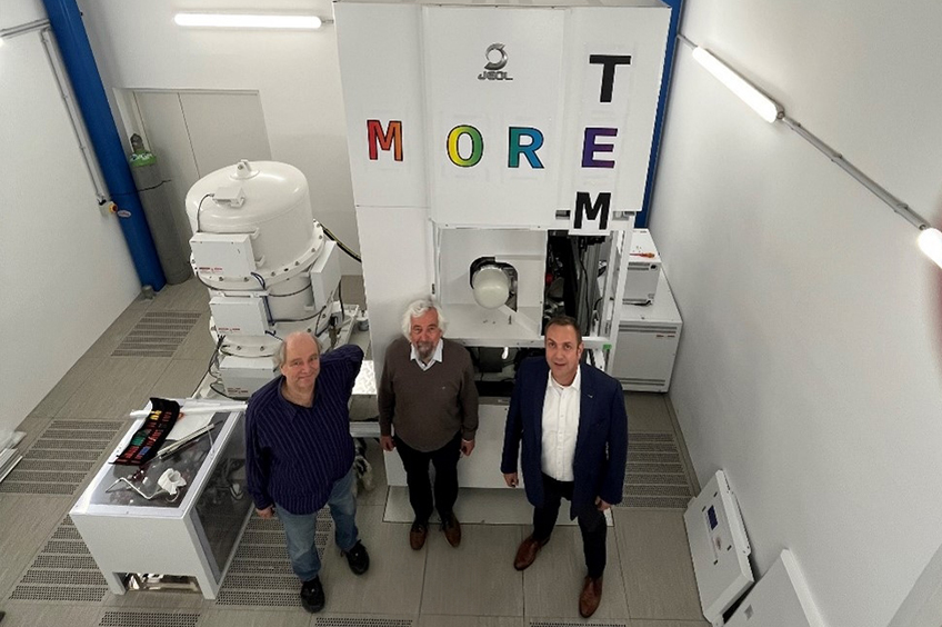
MORE-TEM
MOmentum and position REsolved mapping Transmission Electron energy loss Microscope
MORE-TEM - a revolutionary scientific instrument for materials science
ERC-Synergy Project
1.5.2021- 30.4.2027
A major mission of condensed-matter physics is to understand material properties via the knowledge of the energy vs. momentum (q) dispersion and lifetime of fundamental excitations. Unfortunately, none of the available techniques can be applied to emerging nanomaterials: inelastic x-ray scattering & electron energy loss spectroscopy (EELS) in reflection lack the spatial resolution whereas EELS in transmission electron microscopy lacks the needed combined spatial, energy & q-resolution. In MORE-TEM, we develop a new spectrometer enabling to map excitations q-resolved with 0.01 Å-1 resolution and q-averaged down to atomic level, at unprecedented 1 meV energy resolution and at variable temperature between 700K & 4K. This breakthrough is possible by bringing together our synergy group with complementary skills in electron microscopy, electron optics, experimental & theoretical spectroscopy. This opens the so-far unexplored possibility to investigate dispersion and lifetime of phonons, plasmons & excitons in nanomaterials including (organic) molecules, 1D nanotubes, 2D materials, heterostructures & nanocrystals in minerals with a few nm of lateral resolution on samples as thin as an atomic monolayer. Mapping out the spatial and q-landscape of primary excitations will allow us to gain control on quantum phases, like charge-density waves and superconductivity, to engineer new materials for energy (e.g. batteries), (opto-)electronic devices in (organic) electronics, and to model the physical and chemical properties of natural geological systems. This will hugely impact a wide range of applications in physics, chemistry, engineering, as well as in environmental-, geo- & material science. MORE-TEM not only implements features of a large scale facility on a cheaper table-top instrument, but it also pushes q-resolved spectroscopy to the realm of the nanoscale, providing thus a fundamentally new & unique infrastructure for the characterization and optimization of nanomaterials.
News
Presentation at Expo 2025
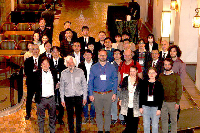
MORE-TEM 2022 Symposium
Synergy Team
PI: Thomas Pichler
PI: Thomas Pichler
University of Vienna, Austria
Co-PI: Francesco Mauri
Co-PI: Francesco Mauri
La Sapienza University, Rome, Italy
Co-PI: Kazu Suenaga
Osaka University, Japan
Co-PI: Max Haider

Co-PI: Max Haider
CEOS GmbH, Heidelberg, Germany
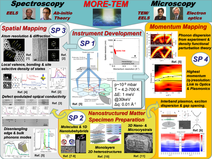
The abovementioned complementary synergy team of experts with expertise in spectroscopy, microscopy and electron optic will develop the MORE-TEM nanospectrometer as “tabletop synchrotron (SP1) to study spatial (SP3) and momentum (SP4) mapping of nanoscale matter specimen (SP2). See sketch below. Figures in the sketch are adapted from the listed references.
References
- Y-C. Lin, S. Morishita, M.Koshino, C-H. Yeh, P-Y. Teng, P-W. Chiu, H. Sawada, and K. Suenaga,
Unexpected Huge Dimerization Ratio in One-Dimensional Carbon Atomic Chains
Nano Letters, 17 (2017) pp.494-500, DOI: 10.1021/acs.nanolett.6b04534 - R. Senga,T. Pichler,K. Suenaga,
Electron Spectroscopy of Single Quantum Objects To Directly Correlate the Local Structure to Their Electronic Transport and Optical Properties
Nano Letters, 16,3661 (2016); DOI: 10.1021/acs.nanolett.6b00825 - R. Senga, T. Pichler, Y. Yomogida, T. Tanaka, H. Kataura, K.Suenaga
Direct Proof of a Defect-Modulated Gap Transition in Semiconducting Nanotubes
Nano Letters, 18,3920 (2018), DOI: 10.1021/acs.nanolett.8b01284 - Y.-C. Lin, P.-Y. Teng, P.-W. Chiu and K. Suenaga
Exploring the single atom spin state by electron spectroscopy
Phys. Rev. Lett., 115 (2015) 206803 DOI: 10.1103/PhysRevLett.115.206803 - R. Senga, K. Suenaga, P. Barone, S. Morishita, F. Mauri, T. Pichler
Position and momentum mapping of vibrations in graphene nanostructures
Nature. 573, 247–250 (2019). https://doi.org/10.1038/s41586-019-1477-8 - J. Hong, R. Senga, T. Pichler, K. Suenaga,
Probing Exciton Dispersions of Freestanding Monolayer WSe2 by Momentum-Resolved Electron Energy-Loss Spectroscopy
Physical Review Letters 124, 087401 (2020); DOI:https://doi.org/10.1103/PhysRevLett.124.087401 - L. Shi, P. Rohringer, K. Suenaga, Y. Niimi, J. Kotakoski, J.C. Meyer, H. Peterlik, M.Wanko, S. Cahangirov, A. Rubio, Z.J. Lapin, L. Novotny, P. Ayala, T. Pichler,
Confined linear carbon chains as a route to bulk carbyne
Nature Materials, 15, 634 (2016); DOI:10.1038/NMAT4617 - H. Shiozawa, A. Briones-Leon, O. Domanov, G. Zechner, Y. Sato, K. Suenaga, T. Saito, M. Eisterer, E. Weschke, W. Lang, H. Peterlik, T. Pichler
Nickel clusters embedded in carbon nanotubes as high performance magnets
Scientific Reports, 5, 15033 (2015); DOI:10.1038/srep15033 - T. Pichler, H. Kuzmany, H. Kataura, and Y. Achiba.
Metallic polymers of C60inside single-walled carbon nanotubes.
Phys. Rev. Lett. 87, 267401 (2001); DOI: 10.1103/PhysRevLett.87.267401. - A.K. Geim, I.V. Grigorieva
Building van der Waals heterostructures.
Nature 499, 419-425 (2013) doi:10.1038/nature12385 - P. Fratzl, R. Weinkamer
Nature’s hierarchical materials
Progress in Materials Science 52,1263–1334 (2007)